Basic material of PCBA
The base material is generally classified by the insulating part of the substrate. The common raw materials are bakelite, glass fiber board, and various plastic boards. And PCB manufacturers generally use an insulating part composed of glass fiber, non-woven material, and resin, and then use epoxy resin and copper foil to make a "prepreg" for use.

The common substrates and main ingredients are:
FR-1-phenolic cotton paper, this substrate is generally called bakelite (higher economy than FR-2)
FR-2-phenolic tissue paper,
FR-3 - Cotton paper (CottON paper), epoxy resin
FR-4 - Woven glass, epoxy resin
FR-5-glass cloth, epoxy resin
FR-6-frosted glass, polyester
G-10--glass cloth, epoxy resin
CEM-1--Tissue paper, epoxy resin (flame retardant)
CEM-2--Tissue paper, epoxy resin (non-flame retardant)
CEM-3--glass cloth, epoxy resin
CEM-4 - Glass cloth, epoxy resin
CEM-5--glass cloth, polyester
AIN -- Aluminum Nitride
SIC - silicon carbide only
Current status of PCBA products
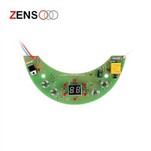
pcba processing

pcba processing
Because the production of PCBA is in the second half of electronic equipment manufacturing, it has become the downstream industry of the electronic industry. almost all electronic
Equipment needs the support of printed circuit boards, so printed circuit boards are the products with the highest market share in the global electronic component products.
Taste. At present, Japan, China, Taiwan, Western Europe and the United States are the main PCB manufacturing bases.
Brief description of PCBA process
SMT and DIP are both ways of integrating parts on the PCB. The main difference is that SMT does not need to drill holes on the PCB, and DIP needs to
The PIN pins of the part are inserted into the already drilled holes.
Circumstances in which PCBA may lead to rejection
Blow hole/pin hole, solder paste return completely, the solder does not wet to the pad or terminal to be soldered, the solder coverage does not meet the requirements, reverse.
Wetting phenomenon results in solder that does not meet surface mount or through-hole solder fillet requirements, and the solder ball violates the minimum electrical clearance and straddles the
Solder connections on conductors that should not be connected, solder bridged to adjacent non-commonly connected conductors or components, solder disturbed, violent, not pressed
It is stipulated that the correct components are selected, the components are not installed in the correct holes, etc.
If you have any different opinions or opinions, you are welcome to leave a message for discussion.